A Three-Stage Comparator and Its Modified Version With Fast Speed and Low Kickback
Also Available Domains Cadence EDA|Tanner EDA
Objective
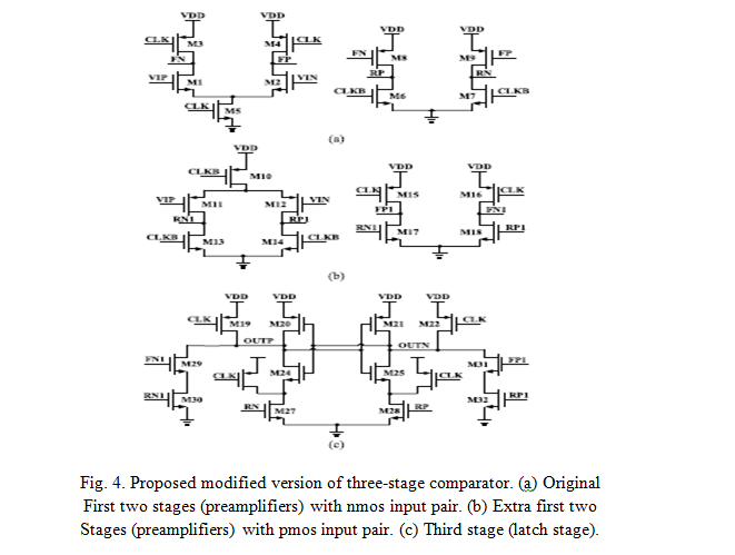
The main aim of this work to reduce the kickback noise and delay in Comparator by using cmos input pair and extra circuitry in latch stage respectively
Abstract
This paper presents a three-stage comparator and its modified version to improve the speed and reduce the kickback noise. Compared to the traditional two-stage comparators, the three-stage comparator in this work has an extra amplification stage, which enlarges the voltage gain and increases the speed. Unlike the traditional two-stage structure that uses pMOS input pair in the regeneration stage, the three-stage comparator makes it possible to use nMOS input pairs in both the regeneration stage and the amplification stage, further increasing the speed. Furthermore, in the proposed modified version of three-stage comparator, a CMOS input pair is adopted at the amplification stage. This greatly reduces the kickback noise by canceling out the nMOS kickback through the pMOS kickback. It also adds an extra signal path in the regeneration stage, which helps increase the speed further. The proposed three-stage comparator and its modified are implemented in 45nm CMOS process in Cadence Virtuoso/Tanner EDA.
NOTE: Without the concern of our team, please don't submit to the college. This Abstract varies based on student requirements.
Block Diagram

Specifications
Software Requirements:
- Cadence Virtuoso/Tanner EDA
- Technology files:45nm
Hardware Requirements:
- Microsoft® Windows XP
- Intel® Pentium® 4 processor or Pentium 4 equivalent with SSE support
- 512 MB RAM
- 100 MB of available disk space
Learning Outcomes
- Introduction to comparators
- Transistors & its applications
- Types of Transistors
- Logic Gates using Transistors
- Pull Up and Pull Down networks
- Importance of Transistors
- MOS Fundamentals
- NMOS/PMOS/CMOS Technologies
- How to design circuits using Transistor logic?
- Transistor level design for comparators
- How to design low power, high speed area efficient transistor level circuits?
- Drawbacks in CMOS technology
- Scope of comparators in today’s world
- Applications in real time
- Cadence Virtuoso/Tanner EDA tool for design and simulation
- Solution providing for real time problems
- Project Development Skills:
- Problem Analysis Skills
- Problem Solving Skills
- Logical Skills
- Designing Skills
- Testing Skills
- Debugging Skills
- Presentation skills
- Thesis Writing Skills


 Paper Publishing
