A Benchmark of Cryo CMOS Embedded SRAM DRAMs in 40 nm CMOS
Objective
This work compares eight different dynamic and static memory cell designs, embedded in identical memory architectures in a nanometer CMOS process typically adopted for QC cryo-CMOS interfaces
Abstract
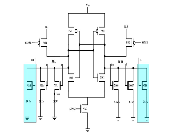
Power consumption is a critical consideration in the design of memory elements and digital systems within very large scale integration (VLSI) circuits. This study introduces a method for reducing power consumption in DRAM sense amplifiers, termed FSPA-VLSA (Foot Switch PMOS Access Voltage Latch Type Sense Amplifier). By implementing this technique within the open bit architecture of DRAM Cells during read operations, an approximate 81% reduction in overall power consumption has been achieved. Additionally, this proposed circuit offers advantages for low-power VLSI/ULSI design. The circuit has been successfully designed and implemented using Cadence Virtuoso tools at 45nm technology.
NOTE: Without the concern of our team, please don't submit to the college. This Abstract varies based on student requirements.
Block Diagram

Specifications
Software Requirements:
· Tool: Cadence virtuoso
· Technology files: GPDK 45nm
Hardware Requirements:
· Microsoft® Windows XP
· Intel® Pentium® 4 processor or Pentium 4 equivalent with SSE support
· 512 MB RAM
· 100 MB of available disk space
Learning Outcomes
- Introduction to Digital electronics
- Importance of Transistors
- MOS Fundamentals
- NMOS/PMOS/CMOS Technologies
- How to design circuits using Transistor logic?
- Scope of DRAM in today’s world
- Use of feedback signals.
- Applications in Real time.
- DRAM importance.
- Solution providing for real time problems
- Project Development Skills:
- Problem Analysis Skills
- Problem Solving Skills
- Logical Skills
- Designing Skills
- Testing Skills
- Debugging Skills
- Presentation skills
- Thesis Writing Skills


 Paper Publishing
