The Mesochronous Dual-Clock FIFO Buffer
Also Available Domains Xilinx Vivado|Xilinx ISE
Objective
This aim of this proposed work is to design a novel mesochronous dual-clock first-input–first-output (FIFO) buffer that can handle both clock synchronization and temporary data storage. Through this design, data is safely transferred on the receiver side of a mesochronous interface without being explicitly synchronized
Abstract
In this project, a novel Mesochronous Dual-clock Buffer is proposed, where the transmitter and receiver modules at the two ends of a Mesochronous interface receive the same clock signal, thus operating under the same clock frequency but have different phase difference. In such cases, clock synchronization is needed when sending data across modules. In this project, we present a novel Mesochronous dual-clock first-input– first-output (FIFO) buffer that can handle both clock synchronization and temporary data storage can be achieved. The proposed design can operate correctly even when the transmitter and receiver are separated by a long link whose delay cannot fit within the target operating frequency. In such scenarios, the proposed Mesochronous FIFO can be extended to support multi-cycle link delays in a modular manner and with minimal modifications to the baseline architecture. The effectiveness of the proposed method is synthesized and simulated using Xilinx ISE 14.7
Keywords: FIFO, Mesochronous FIFO, synchronous FIFO butter
NOTE: Without the concern of our team, please don't submit to the college. This Abstract varies based on student requirements.
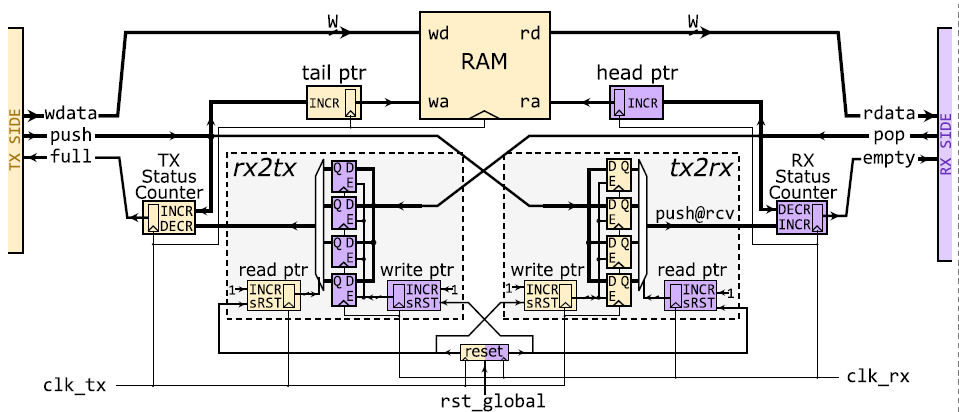
Block Diagram
Specifications
Software Requirements:
- Xilinx ISE 14.7/Xilinx Vivado
- HDL: Verilog
Hardware Requirements:
- Microsoft® Windows XP
- Intel® Pentium® 4 processor or Pentium 4 equivalent with SSE support
- 512 MB RAM
- 100 MB of available disk space
Learning Outcomes
- Basics of Digital Electronics
- FPGA design Flow
- Introduction to Verilog Coding
- Different modeling styles in Verilog
- Data Flow modeling
- Structural modeling
- Behavioral modeling
- Mixed level modeling
- Combinational & Sequential circuits
- Knowledge on FIFO
- Clock Synchronization
- Different synchronization methods
- Loosely Coupled
- Tightly Coupled
- About buffering Architecture
- Data transferring at different conditions
- About RAM
- Applications in real time
- Xilinx ISE 14.7/Xilinx Vivado for design and simulation
- Generation of Netlist
- Solution providing for real time problems
- Project Development Skills:
- Problem Analysis Skills
- Problem Solving Skills
- Logical Skills
- Designing Skills
- Testing Skills
- Debugging Skills
- Presentation Skills
- Thesis Writing Skills
Demo Video


Request for Video
 Paper Publishing
Request Call Back
Would you like to receive a free callback now?
Choose the best time for callback:
Leave your message and we will contact you as soon as possible

6-2-85/B, Old Maternity Hospital Road, Thyagaraja Nagar, Tirupati, Andhra Pradesh – 517501
+91 9030333433
+91 9393939065
0877-2261612

Disclaimer - Takeoff Edu Group Projects are not associated or affiliated with IEEE in any way. The IEEE Projects mentioned here are mentioned in the context of student projects, whose ideas are derived from IEEE publications, not projects of or by IEEE.